半导体BCD(Bipolar-CMOS-DMOS)工艺是一种集成电路制造技术,它将双极型晶体管(Bipolar)、互补金属氧化物半导体(CMOS)和双扩散金属氧化物半导体(DMOS)三种不同类型的晶体管集成在同一块芯片上。这种工艺结合了双极型晶体管的较高电流驱动能力和CMOS电路的低功耗特点,以及DMOS器件的高电压、大电流处理能力。
以下是BCD工艺的主要特点和应用:
1. 双极型晶体管(Bipolar):用于模拟电路和高电流应用,因为它们可以提供较高的电流增益。
2. 互补金属氧化物半导体(CMOS):用于数字逻辑电路,因为它们具有低功耗和高集成度的特点。
3. 双扩散金属氧化物半导体(DMOS):用于功率电子器件,如高压或大电流开关,因为它们能够处理较高的电压和电流。
BCD工艺的关键优势包括:
1.多功能性:可以在同一芯片上集成多种功能,如模拟、数字和功率电路。
2.能效:结合了双极型晶体管和CMOS的优点,可以实现能效较高的电路设计。
3.集成度:高集成度减少了芯片面积,降低了成本。
4.性能:能够提供高电流驱动能力和处理高电压的能力。
BCD工艺广泛应用于以下领域:
1.汽车电子:汽车中的电源管理、电机控制、车身电子和娱乐系统。
2.消费电子:如智能手机、平板电脑和其他便携式设备中的电源管理。
3.工业应用:工业自动化、电力电子和控制系统。
随着技术的发展,BCD工艺也在不断进步,如BCD5、BCD6等,这些工艺提供了更高的电压和功率处理能力,以及更好的性能和能效。
| ● Available ★Indude SOI Process |
| Tech. |
BCD |
HV CMOS |
Mixed-Signal |
Logic |
e-NVM |
| 0.13μm/0.11μm |
● |
|
|
● |
● |
| 0.18μm/0.153μm |
● |
● |
● |
● |
● |
| 0.25μm |
● |
|
● |
|
|
| 0.35μm |
|
|
● |
● |
● |
| 0.5μm |
● ★ |
● |
● |
● |
● |
| >0.5μm |
|
● |
● |
● |
|
| >1.0μm |
|
● |
● |
● |
|
| MEMS |
Pressure sensor,Microphone sensor,Photoelectric MEMS and Thermopiles sensor are available.
Accelerometer,Gas sensorand Micro-mirrorare under development. |
| Special Device |
APD/SPAD are underdevelopment. |
| ★Advanced BCD Available ▲Advanced BCD Developing ●HV /UHV BCDAvailable ⊙Include SOI Process |
| |
0.11μm |
0.153μm |
0.18μm |
0.25μm |
0.5μm |
0.8μm |
1.0μm |
| 12V |
★ |
★ |
★ |
★ |
|
|
|
| 18V |
★ |
★ |
★ |
★ |
|
|
|
| 24V |
★ |
★ |
★ |
★ |
|
|
|
| 30V |
★ |
★ |
★ |
★ |
|
|
|
| 40V |
|
★ |
★ |
★ |
|
● |
● |
| 60V |
|
|
★ |
★ |
|
|
|
| 80V |
|
|
★ |
|
|
|
|
| 120V |
|
|
★ |
|
●⊙ |
|
|
| 200V |
|
|
▲ |
|
●⊙ |
● |
● |
| 600V |
|
|
|
|
●⊙ |
● |
● |
| 700V |
|
|
|
● |
|
● |
● |
| 1200V |
|
|
|
|
|
● |
|
联系人:谢工
电话:+86 138 2505 8605 (微信同号)
邮箱:sales@plutosemi.com
xie.lance@qq.com
------------------------------------------------------------------------------------------------------------------------------------
Chip Foundry
Pluto provides chip foundry service with close collaboration with whole world customers and the assurance that intellectual property is protected and respected.
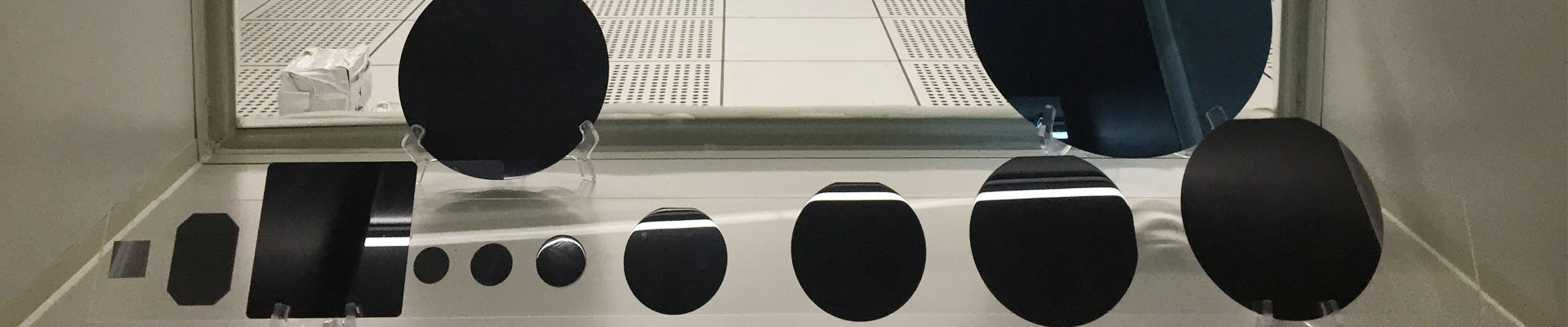
Pluto was known as PLUTOSEMI, a famous substrate manufacturer and solution provider, and has been operating for 10+ years. Our Chip foundry provides 6” (150mm) and 8” (200mm) wafer lines. we have 300 state-of-the-art semiconductor processing tools has marked a key milestone in our chip Foundry transformation. It has expanded Pluto’s capability to develop and manufacture sophisticated microdevices, biochips, and sensors.
Have your custom products outgrown the university environment, or do you require a level of customization at lower volumes that is not always supported in pure-play semiconductor foundries? Our team of experienced process engineers can help you manufacture your custom projects on 150- or 200-mm wafer diameters. We offer core competencies in the following areas:
· CMOS
· Bipolar-CMOS-DMOS (BCD)
· Embedded Nonvolatile Memory (eNVM)
· Silicon-on-Insulator (SOI) high-voltage technologies
· Charge Coupled Devices (CCDs)
· Micro-Electrical Mechanical Systems (MEMS)
The semiconductor BCD (Bipolar-CMOS-DMOS) process is an integrated circuit manufacturing technology that integrates three different types of transistors—bipolar transistors (Bipolar), complementary metal-oxide-semiconductors (CMOS), and double diffused metal-oxide-semiconductors (DMOS)—onto a single chip. This process combines the high current driving capability of bipolar transistors with the low power consumption characteristics of CMOS circuits, as well as the high voltage and large current handling capabilities of DMOS devices.
The main features and applications of the BCD process are as follows:
1、Bipolar transistors (Bipolar): Used in analog circuits and high current applications because they can provide higher current gain.
2、Complementary metal-oxide-semiconductors (CMOS): Used in digital logic circuits due to their low power consumption and high integration.
3、Double diffused metal-oxide-semiconductors (DMOS): Used in power electronic devices, such as high voltage or large current switches, because they can handle higher voltages and currents.
The key advantages of the BCD process include:
1、Versatility: Multiple functions, such as analog, digital, and power circuits, can be integrated on the same chip.
2、Energy efficiency: By combining the advantages of bipolar transistors and CMOS, it achieves circuit designs with higher energy efficiency.
3、Integration: High integration reduces the chip area and lowers costs.
4、Performance: It can provide high current driving capability and the ability to handle high voltages.
The BCD process is widely used in the following fields:
1、Automotive electronics: Power management, motor control, body electronics, and entertainment systems in cars.
2、Consumer electronics: Power management in smartphones, tablets, and other portable devices.
3、Industrial applications: Industrial automation, power electronics, and control systems.
As technology advances, the BCD process is also evolving, with developments like BCD5, BCD6, etc., offering higher voltage and power handling capabilities, as well as improved performance and energy efficiency.
| ● Available ★Indude SOI Process |
| Tech. |
BCD |
HV CMOS |
Mixed-Signal |
Logic |
e-NVM |
| 0.13μm/0.11μm |
● |
|
|
● |
● |
| 0.18μm/0.153μm |
● |
● |
● |
● |
● |
| 0.25μm |
● |
|
● |
|
|
| 0.35μm |
|
|
● |
● |
● |
| 0.5μm |
● ★ |
● |
● |
● |
● |
| >0.5μm |
|
● |
● |
● |
|
| >1.0μm |
|
● |
● |
● |
|
| MEMS |
Pressure sensor,Microphone sensor,Photoelectric MEMS and Thermopiles sensor are available.
Accelerometer,Gas sensorand Micro-mirrorare under development. |
| Special Device |
APD/SPAD are underdevelopment. |
| ★Advanced BCD Available ▲Advanced BCD Developing ●HV /UHV BCDAvailable ⊙Include SOI Process |
| |
0.11μm |
0.153μm |
0.18μm |
0.25μm |
0.5μm |
0.8μm |
1.0μm |
| 12V |
★ |
★ |
★ |
★ |
|
|
|
| 18V |
★ |
★ |
★ |
★ |
|
|
|
| 24V |
★ |
★ |
★ |
★ |
|
|
|
| 30V |
★ |
★ |
★ |
★ |
|
|
|
| 40V |
|
★ |
★ |
★ |
|
● |
● |
| 60V |
|
|
★ |
★ |
|
|
|
| 80V |
|
|
★ |
|
|
|
|
| 120V |
|
|
★ |
|
●⊙ |
|
|
| 200V |
|
|
▲ |
|
●⊙ |
● |
● |
| 600V |
|
|
|
|
●⊙ |
● |
● |
| 700V |
|
|
|
● |
|
● |
● |
| 1200V |
|
|
|
|
|
● |
|
Sales Engineer:Lance Xie
Phone:+86 138 2505 8605
Email:sales@plutosemi.com
xie.lance@qq.com