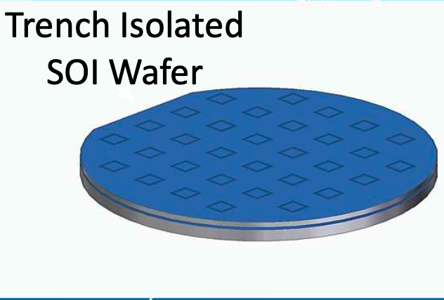

| Parameter | Specification Range |
| Wafer Diameter | 100, 125, 150 mm |
| Handle Layer Specifications | |
| Handle Thickness | 350–800 μm |
| Handle Thickness Tolerance | ±5 μm |
| Stack Thickness | 350–1150 μm |
| Dopant Type | N or P |
| Doping | N type: Phos, Red Phos, Sb & As P type: Boron |
| Resistivity | ≤0.001 – ≥10000 Ω-cm |
| Growth Method | CZ, MCZ or FZ |
| Crystal Orientation | <100>, <111> or <110> |
| Backside Finish | Lapped/Etched or Polished |
| Buried Oxide Specifications | |
| Thermally Oxidised Buried Oxide Thickness | 0.2 – 4.0 μm grown on Handle, Device or both wafers |
| Device Layer Specifications | |
| Device Layer Thickness | 1.5 - 100 μm |
| Tolerance | ± 0.5 μm |
| Dopant Type | N or P |
| Doping | N type: Phos, Red Phos, Sb & As P type: Boron |
| Resistivity | ≤0.001 – ≥10000 Ω-cm |
| Growth Method | CZ, MCZ or FZ |
| Crystal Orientation | <100>, <111> or <110> |
| Buried Layer Implant | N type or P type |
| Trench Mask Tone | Positive Resist |
| Trench Mask Type | E-beam master for projection aligner |
| Trench Line Width | > 2um |
| Trench Aspect Ratio | 15:01 |
| Trench Sidewall Doping Type | Phosphorus |
| Trench Refill – Oxide (each sidewall) | 0.1 – 1.0 μm |
| Trench Refill – Polysilicon | To Fill (Doped or undoped Polysilicon) |
| Planarisation | CMP |
| Final Field Oxide | Thermal oxide + TEOS up to 1um |
